-
Mail us
sale@tiger-transformer.com -
Phone us
(+86)15155183777 -


Mail us
sale@tiger-transformer.comPhone us
(+86)15155183777
Classification of network transformers
Can be divided into two categories: a. Discrete LAN Magnetics Module; b. RJ45 Connector with Integrated Magnetics, ICMs );
Products can be divided into two categories according to customer welding type: a. Surface mount components (SMT, Surface Mount Type) b. Plug-in components (TH, Through-Hole Type)
Products can be classified into four categories based on transmission rate: a.10Base-T, b.10/100Base-T, c.1000 Base-T, d.10G Base-T.
(Base -T: Baseband, twisted pair. In short, Base-T is a local area network (LAN) standard that operates at bps rate. It is often called Fast Ethernet and uses UTP (Unshielded Twisted Pair) ) copper cable. There are three basic implementations of Fast Ethernet: Base-FX, Base-T, and 1Base-T4. Each specification is identical except for the interface circuitry, which determines which type they use cable. In order to implement the clock/data recovery (CDR) function, Base-T uses the 4B/5B Manchester Encoding mechanism.)
1. Common mode choke (CMC: Common mode Choke)
Common mode choke , also called common mode choke inductor, is a closed magnetic ring with coils wound in opposite directions and with the same number of turns symmetrically. An ideal common mode choke has the function of inhibiting the common mode interference between L (or N) and E, but has no inductive effect on the differential mode interference existing between L and N. However, the incomplete symmetry of the actual coil winding will lead to the generation of differential mode leakage inductance. Signal current or supply current flows in opposite directions in the two windings, the resulting magnetic fluxes cancel each other out, and the choke exhibits low impedance. Common-mode noise currents (including disturbance currents caused by ground loops, also called longitudinal currents) flow in the same direction through the two windings. The generated magnetic fluxes add in the same direction, and the choke coil exhibits high impedance, thus suppressing the common mode noise current. The effect of modulo noise. The common mode inductor is essentially a two-way filter: on the one hand, it must filter out common mode electromagnetic interference on the signal line; on the other hand, it must suppress itself from emitting electromagnetic interference to avoid affecting the normal operation of other electronic equipment in the same electromagnetic environment. .
Common mode chokes can transmit differential mode signals. Both DC and differential mode signals with very low frequency can pass through. However, high-frequency common mode noise presents a large impedance, so it can be used Suppress common mode current disturbance.
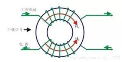
Common mode inductor choke is a switching power supply, variable frequency It is an important part of equipment such as controllers and UPS power supplies. Its working principle: When the working current flows through two coils with opposite winding directions, two mutually canceling magnetic fields H1 and H2 are generated. At this time, the working current is mainly damped by the ohmic resistance of the coil and the small leakage inductance at the negligible operating frequency. . If an interference signal flows through the coil, the coil will exhibit high impedance, producing a strong damping effect to attenuate the interference signal.
CMC suppresses common-mode signals:
As the name suggests, common-mode chokes are components used to suppress common-mode noise signals (useless signals, interference signals). The noise signal forms a high impedance and has basically no effect on the differential mode signal (the useful signal). It is the main component that suppresses EMI electromagnetic interference. Its working principle is as follows:
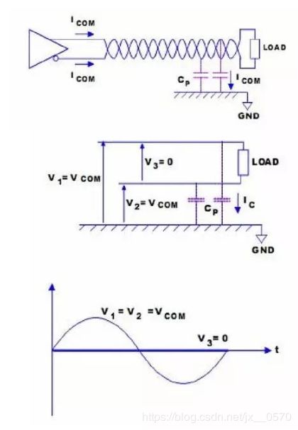
Common mode signal refers to a signal with the same polarity input at both input terminals. Common mode signals will cause electromagnetic interference. Electromagnetic interference is divided into radiated interference and conducted interference (entering the power line). Asymmetric signal transmission and differential-mode signal conversion during impedance mismatch will produce common-mode signals in digital terminal equipment.
CMC has no effect on differential mode signals:
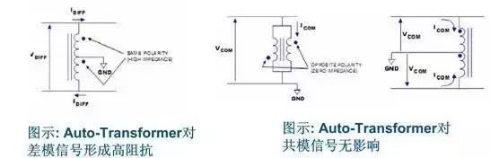
2. Self-coupling transformer (Center Tapped Auto-Transformer)
The self-coupling transformer forms a high impedance for differential mode signals and basically has no effect on common mode signals. It should be connected according to the above wiring method. In the line, signals can be transmitted effectively, thereby further reducing and suppressing electromagnetic interference.
3. Working principle and insertion loss characteristics of choke coil (or impedance characteristics):
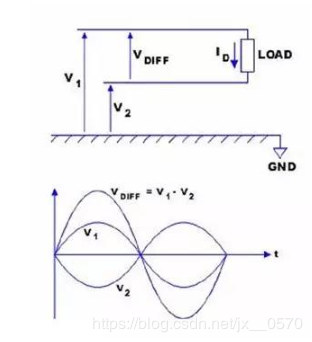
When a signal voltage (differential mode signal) is applied to the two legs of the transformer, an induced voltage is induced at the secondary end of the transformer through magnetic circuit coupling. Regarding the signal voltage, since the signal currents flowing through the two windings of the CMC at the same time are equal in magnitude and opposite in direction, magnetic fluxes in opposite directions are generated in the core magnetic circuit of the CMC, which cancel each other out and do not affect differential mode signal transmission. At this time, currents of equal size and direction flow through the two windings of the Transformer, causing the Transformer to act like a large resistor, hindering the passage of differential mode signals and having little impact on the transmission of carrier signals.
So the differential mode signal is directly coupled to the load. For common mode signals, they are mainly coupled to the secondary through the distributed capacitance between the primary and secondary of the transformer. At this time, the two windings of the CMC flow with currents of equal magnitude and direction. At this time, the CMC is equivalent to a A large resistor prevents the transmission of common-mode current, while the two windings of the transformer flow with equal and opposite currents, which is equivalent to a short circuit for the common-mode signal. In this way, the common-mode voltage will basically not be transmitted, but will be coupled. onto the load. In this way, the carrier signal can be transmitted well and the common mode interference signal can be suppressed.
The center tap of the transformer. Why are some of the center taps connected to the power supply? Somewhat grounded? This is mainly determined by the UTP (twisted pair) port driver type of the phy chip used. There are two types. If it is voltage driven, it must be connected to the power supply; if it is current driven, it is not needed and a capacitor is directly connected to the ground. Why are some connected to 2.5v? And some are connected to 3.3v? This is determined by the UTP port level specified in the PHY chip data. If it is 2.5v, pull it up to 2.5v, if it is 3.3v, pull it up to 3.3v.
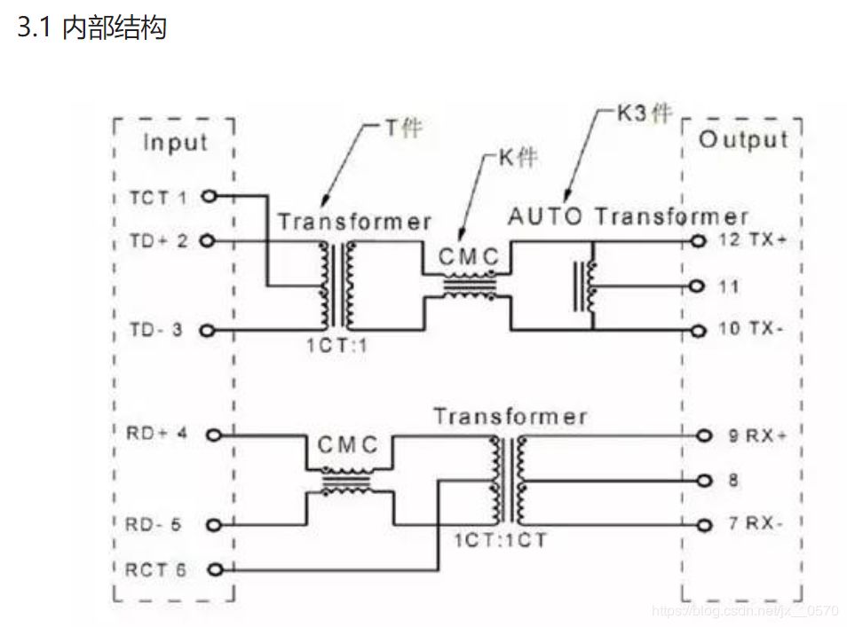
1 The function of the network port transformer
1. Why are some of the middle taps connected to the power supply? Somewhat grounded?
This is mainly determined by the UTP port driver type of the PHY chip used. There are two types of drivers, voltage driver and current driver. If it is driven by voltage, it needs to be connected to the power supply; if it is driven by current, just connect a capacitor directly to the ground! Therefore, for different chips, the connection method of the center tap is closely related to the PHY. For details, please refer to the chip's datasheet and reference design.
2. Why are the voltages connected to different voltages when connected to the power supply?
This is also determined by the UTP port level specified in the PHY chip data used. Whatever level you decide, you have to connect the corresponding voltage. That is, if it is 2.5v, pull it up to 2.5v, if it is 3.3v, pull it up to 3.3v.
3. What is the function of this transformer? Can it be left unconnected?
Theoretically, it is possible to connect it directly to the RJ45 without a transformer, and it will still work normally. However, the transmission distance is very limited, and it will also be affected when connected to network ports of different levels. Moreover, external interference to the chip is also great. When the network transformer is connected, it is mainly used for signal level coupling. First, it can enhance the signal and make it transmit farther; second, it isolates the chip end from the outside, greatly enhances the anti-interference ability, and adds a great protection to the chip (such as lightning strikes); third, when connected When connecting to network ports with different levels (for example, some PHY chips are 2.5V and some PHY chips are 3.3V), they will not affect each other's equipment.
In general, network transformers mainly play the functions of signal transmission, impedance matching, waveform repair, signal clutter suppression and high voltage isolation.
Data mercury is also called a network transformer or a network isolation transformer. It plays two main roles on a network card. One is to transmit data. It filters the differential signal sent out by the PHY with differential mode coupling coil coupling to enhance the signal, and couples it to different levels through electromagnetic field conversion. Connect the other end of the network cable; first, isolate the different levels between different network devices connected by the network cable to prevent different voltages from being transmitted through the network cable and damaging the equipment. In addition, data mercury can also play a certain role in lightning protection for equipment.
When a signal voltage (differential mode signal) is applied to the two legs of the transformer, an induced voltage is induced at the secondary end of the transformer through magnetic coupling. Regarding the signal voltage, since the signal currents flowing through the two windings of the CMC at the same time are equal in magnitude and opposite in direction, magnetic fluxes in opposite directions are generated in the core magnetic circuit of the CMC, which cancel each other out and do not affect differential mode signal transmission.
At this time, the currents of equal size and direction flow through the two windings of the CMT, causing the CMT to act like a large resistor, hindering the passage of differential mode signals and affecting the transmission of carrier signals. Very rarely. So the differential mode signal is directly coupled to the load. For common mode signals, they are mainly coupled to the secondary through the distributed capacitance between the primary and secondary of the transformer. At this time, the two windings of the CMC flow with currents of equal magnitude and direction. At this time, the CMC is equivalent to a A large resistance prevents the transmission of common-mode current, while the two windings of the CMT flow with equal and opposite currents, which is equivalent to a short circuit for the common-mode signal. In this way, the common-mode voltage will basically not be transmitted, but will be coupled to on load. In this way, the carrier signal can be transmitted well and the common mode interference signal can be suppressed.
PHY’s DAC (Digital to Analog Converter) does have voltage drive and current drive. The specific details really depend on the PHY’s DATASHEET. But regardless of voltage drive or current drive, the center tap of the PHY side transformer must be connected to a capacitor for filtering.
The important thing is that for current-driven PHY, the 2-wire CMC (COMMON MODE CHOKE) line at the PHY end is not applicable, because the current may saturate the CMC and cause it to lose its common mode suppression effect. But the 3-wire CMC line on the PHY end is fine because the third line is equivalent to an autotransformer in principle. However, under the general winding method, the common mode suppression capability of the 2-wire CMC is better than that of the 3-wire CMC.
The reason is that there is magnetic field cancellation in the 3-wire CMC. However, a special winding method can avoid this shortcoming, but I am unable to disclose it here because it involves patent issues. In addition, the 3-wire CMC line can provide more line balance, so its conversion characteristics of different mode signals are better. If there is a margin for EMI (interference) but there is a problem with EMS (anti-interference), you should consider using a 3-wire CMC. of transformers. On the other hand, if EMS has margin but EMI is a problem, use a transformer with 2-wire CMC. If there is no margin for both, then you need to discuss improvement measures with your supplier in detail.
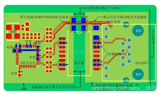
a) Keep the distance between RJ45 and transformer as much as possible The crystal oscillator should be kept away from interfaces, PCB edges and other high-frequency devices, traces or magnetic components. The distance between the PHY layer chip and the transformer should be as short as possible. However, sometimes in order to take into account the overall layout, this may be difficult to meet. However, the distance between them is about 10~12cm at most. The principle of device layout is that it is usually placed according to the signal flow direction and must not go around;
b) The power filtering of the PHY layer chip is designed according to the requirements of the chip. , usually a decoupling capacitor needs to be placed at each power supply terminal. They can provide a low-impedance path for the signal and reduce the resonance between the power supply and the ground plane. In order for the capacitor to play the role of decoupling and bypass, it must be ensured The decoupling and bypass capacitor loop area composed of capacitors, wiring, vias, and pads should be as small as possible to ensure that the lead inductance is as small as possible;
c) The center tap pair on the chip side of the network port transformer PHY layer The ground filter capacitor should be as close as possible to the transformer pin to ensure the shortest lead and the smallest distributed inductance;
d) The common mode resistor and high voltage capacitor on the interface side of the network port transformer should be placed close to the center tap, with short and thick traces (≥15mil);
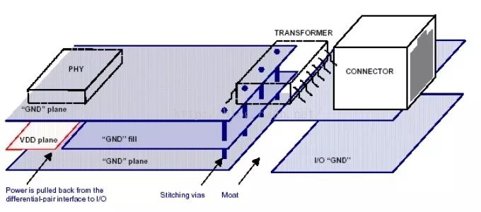
e) Both sides of the transformer need to be grounded: that is, the RJ45 connector and the secondary coil of the transformer use separate isolated grounds. The isolation area is more than 100mil, and there is no power and power supply in this isolation area. strata exist. This separation process is to achieve isolation between the primary and secondary, and the interference from the control source is coupled to the secondary through the reference plane;
f) The power line of the indicator light and the drive signal line are routed adjacently. Minimize loop area as much as possible. Necessary isolation must be carried out between the indicator light and the differential line, and sufficient distance must be maintained between the two. If there is space, it can be separated by GND;
g) The resistors and capacitors used to connect GND and PGND need to be placed and separated area.
2. Ethernet signal lines exist in the form of differential pairs (Rx±, Tx±). The differential lines have strong common-mode suppression capabilities and strong anti-interference capabilities. However, if the wiring is improper, the Will cause serious signal integrity problems. Let's introduce the key points of differential line processing one by one:
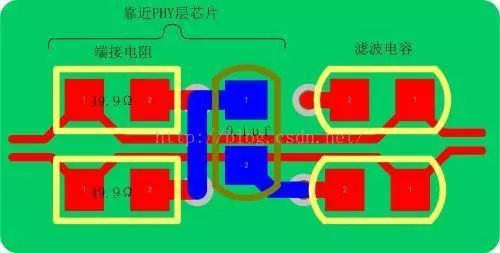
a) Prioritize drawing Rx±, Tx± differential pairs, try to keep the differential pairs parallel, equal length, and short distance, and avoid via holes and crossovers. Due to factors such as pin distribution, vias, and wiring space, differential line lengths are prone to mismatch, timing will be offset, and common-mode interference will be introduced, reducing signal quality. Therefore, it is necessary to compensate for the mismatch of the differential pair so that the line lengths match. The length difference is usually controlled within 5 mil. The compensation principle is to compensate where the length difference occurs;
b) When the speed When the requirements are high, it is necessary to control the impedance of the Rx± and Tx± differential pairs. Usually the impedance is controlled at 100Ω±10%;
c) Differential signal terminal resistor (49.9Ω, some PHY layer chips may not have it) It must be placed close to the Rx± and Tx± pins of the PHY layer chip, so as to better eliminate signal reflection in the communication cable. Some of this resistor is connected to the power supply, and some is connected to the ground through the capacitor. This is determined by the PHY chip;
d) The filter capacitors on the differential line pairs must be placed symmetrically, otherwise the differential mode may be converted into common mode, causing common mode noise, and there must be no stubs in the wiring, so as to have good protection against high-frequency noise. Inhibition ability.
3. Transformer integrated in the connector of the Ethernet circuit The PCB layout and wiring are much simpler than those without integration. Figure 3 below is the PCB layout and wiring reference diagram of the network port circuit using integrated connectors:
Figure 3 Network port PCB layout and wiring reference diagram of the integrated connector
As can be seen from the above picture The difference between Figure 3 and Figure 1 is that the network port transformer is missing, and the other two are roughly the same. The main difference is that the network port transformer has been integrated into the connector, so the ground plane does not need to be divided, but we still need to connect the shell of the integrated machine to a continuous ground plane.
4. Circuit filter design:
a) Connect 10R resistors in series to the differential lines, and add 5-10pF capacitors to ground respectively
b) Add LC filtering to the transformer power supply, select 600R/100Mhz magnetic beads and 0.01-0.1uF capacitor
5. Circuit lightning protection design:
In order to meet IEC61000-4-5 or GB17626.5 Standard, common mode 2KV, differential mode 1KV lightning protection test requirements, the lowest cost design solution is that the primary center tap of the transformer is grounded through the lightning protection device, you can choose a lower cost semiconductor discharge tube, but pay attention to the "nominal voltage of the protection device" The requirement is greater than or equal to 6V; the peak current requirement of the protective device is greater than or equal to 50A; the peak power requirement of the protective device is greater than or equal to 300 W. Pay attention to the selection of semiconductor discharge tubes, and note that the "off-state voltage and holding current" of the device must be greater than the circuit operating voltage and operating current.
According to the test standard requirements, for unshielded balanced signals, differential mode testing is not required to be mandatory. Therefore, for protection requirements within differential mode 1KV, the energy impact can be protected through the transformer's own winding. Differential mode protection devices need to be added.
1) Since the TVS tube responds faster than the varistor and the gas discharge tube, the varistor or gas discharge tube cannot be used directly in parallel with the TVS tube. Instead, a uH level inductor or inductor should be connected in series between them. Wires (wires also have parasitic inductance);
2) The gas discharge tube needs freewheeling interruption: that is, it must be able to return to the open circuit state after absorbing the transient and causing a short circuit, that is, in general use, the gas discharge tube needs The DC breakdown voltage is much higher than the working voltage of its parallel signal. When the gas discharge tube acts due to transient interference and a short circuit occurs, a voltage is required to maintain the short circuit state. If the signal voltage will keep the gas discharge tube at In the short-circuit state, the signal will be burned over time, so the signal voltage must be lower than the voltage that maintains the short-circuit state of the gas discharge tube.
Radiation and ESD:
a) Add magnetic beads to the indicator light wiring and power supply, and place the magnetic beads close to the interface, and then The current limiting resistor is placed close to the PHY chip and capacitive filtering is added.
PCB layout and routing principles:
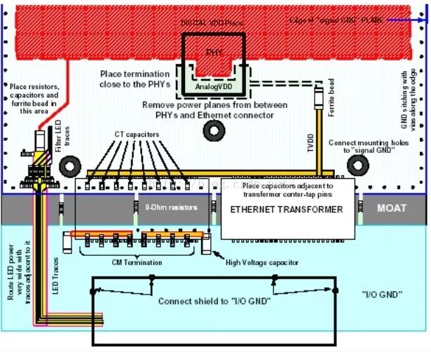
1) Between the transformer and RJ45, the distance between the PHY layer chip and the transformer should be controlled within 1 inch. When layout conditions are limited, priority should be given to ensuring that the distance between the transformer and RJ45 is within 1 inch.
2) The device layout should be placed according to the signal flow direction, and do not go around.
3) The ground plane under the transformer should be divided, the width of the dividing line should not be less than 100MIL, and the network port transformer should be placed on the dividing line between GND and PGND.
4) Each pair of differential traces must be controlled to have the same length, and the impedance should be controlled to 50 ohms.
5) Note that the digital ground and analog ground of the PHY layer chip are unified, and the digital power supply and analog power supply are isolated using magnetic beads. At the same time, it must be coordinated with the transformer. Pay attention to the power filtering of the PHY chip and design it according to the chip requirements.
6) The 3.3V or 2.5V power line of the network port indicator light comes from the power plane. They must be decoupled using magnetic beads and capacitors; the indicator drive line must be close to the PHY series resistor and Perform capacitive filtering before entering the I/O area. This prevents noise from coupling into the differential pair area through the indicator power lines.
7) The indicator power line and drive signal line should be close to the wiring to minimize the loop area.
8) The indicator line and the differential line pair must be isolated as necessary. The distance between the two must be far enough. If necessary, use a GND plane for isolation.
9) Note that the filter capacitor from the center tap of the chip side of the network port transformer to the ground should be as close as possible to the transformer pin to ensure the shortest lead and the smallest distributed inductance.
10) The 0 ohm resistor or capacitor used to connect GND and PGND should be placed on the ground dividing line.
11) The analog power supply of the PHY chip should not occupy a large area of plane. It is pulled from the local copper through traces, magnetic beads, and traces to the center tap on the transformer chip side.
12) There is no VDD between the PHY chip and the transformer. Define the plane layer area between the PHY chip and the transformer as GND, which can cut off the noise path from the VDD plane.
13) Along the edge of the single-board PCB (no need to wrap PGND, see Figure 8) Drill a ground via every 250 mil. These rows of vias can cut off the way the single board noise radiates outward and reduce the impact on the PGND static ground.
14) The PGND and GND of the single board are connected to the structure through the screw holes to ensure the unity of the system ground potential.
15) Ensure good decoupling (low resistance) between the power plane and the ground plane. The power plane is preferably adjacent to the ground plane.
16) The signal lines adjacent to the power plane should not exceed the projection area of the power plane.
17) Ensure the integrity of the return path of the signal line adjacent to the power plane, otherwise the shape of the plane will be changed so that the signal line is in the plane layer, and the incomplete return path will cause Come to serious EMC problems.
18) It is recommended that all high-speed signal lines, I/O lines, and differential line pairs be routed close to the ground plane first. If this is not possible, use the power plane as the reference plane.
19) Differential lines should be kept away from other signal lines, and other signal lines should be placed to couple noise to the differential lines.
20) In order to reduce the noise of differential signals, digital signal lines or power supplies should be kept away from analog signal lines or power supplies.
21) Decoupling and bypassing of the power supply are very important. They can provide a low-impedance path for the signal and reduce the resonance between the power supply and the ground plane. Capacitors can play the role of decoupling and bypass, but it is necessary to ensure that the area of the decoupling and bypass capacitor loop composed of capacitors, traces, vias, and pads is as small as possible, and the lead inductance must be as small as possible, see the figure below Shown
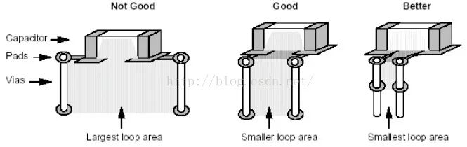
The loop area of the decoupling capacitor
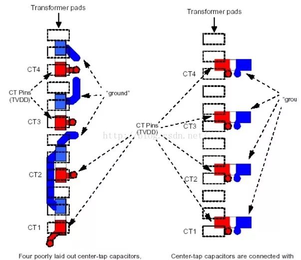
Layout and wiring comparison diagram of transformer center tap common mode capacitor
7.2. PCB layout and wiring rules for network port circuits using integrated connectors
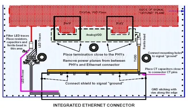
Only the differences are described below.
1) The network port transformer is an isolation device used to cut off the common mode. Because it has been integrated into the connector, the ground plane is no longer divided.
2) The housing of the integrated connector should be connected to a continuous ground plane. Do not create rack ground underneath the connector.
3) Drill grounding vias every 250 mil around the board to shield the board noise within the board.
A very important point (drawing reference from computer motherboard design): The metal casing of grounding equipment exposed outside the chassis needs to be protected against contact discharge (such as 232 USB Ethernet interface, etc.), and their signal lines must be protected Measures such as GDT pressure-sensitive TVS, etc. should be connected to the metal shell, which is the earth, and discharged to the earth (the metal shell of grounding equipment is generally connected to the earth).