-
Mail us
sale@tiger-transformer.com -
Phone us
(+86)15155183777 -


Mail us
sale@tiger-transformer.comPhone us
(+86)15155183777
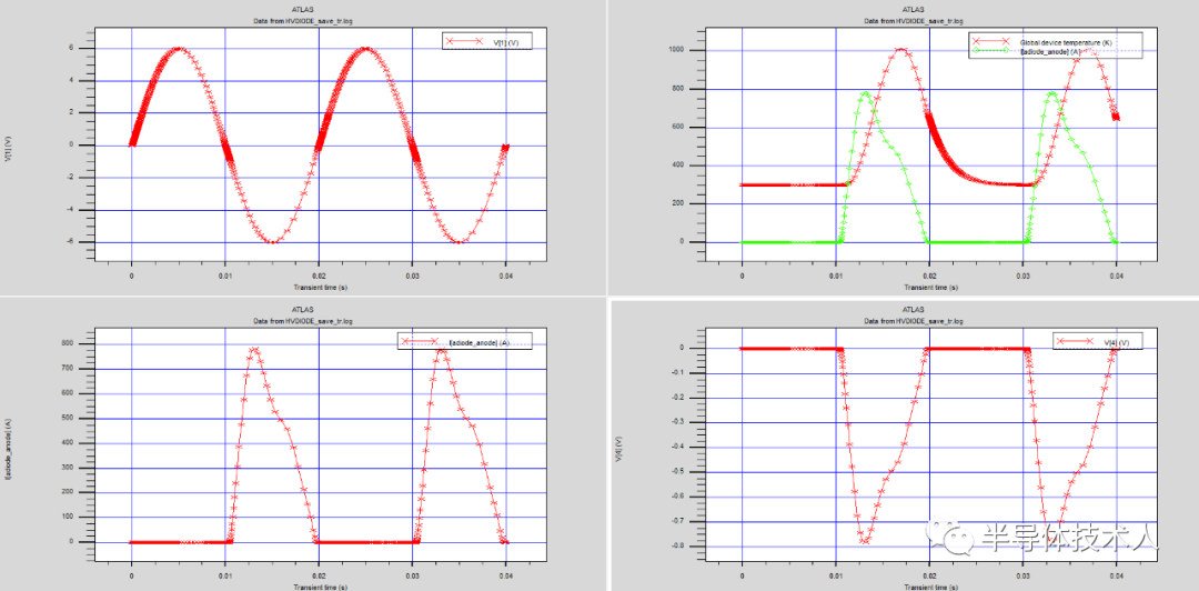
(1)VP=6V
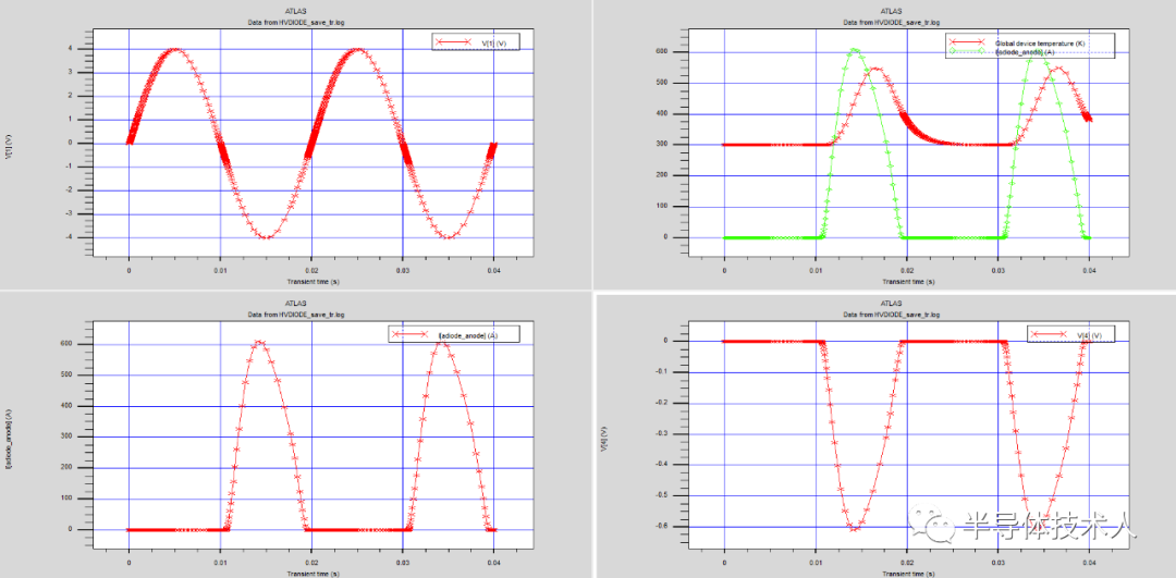
(2)VP=4V
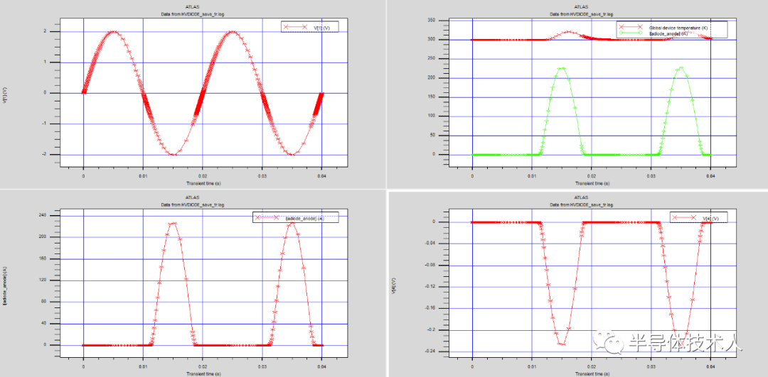
(3)VP=2V
################################ #########################
Conduction angle: The conduction angle is the Inside, the conduction angle is controlled by the power electronic device. Alternating current is generally a sinusoidal waveform, and its cycle is 360 degrees, the positive half cycle accounts for 180 degrees, and the negative half cycle accounts for 180 degrees. When the alternating current passes through the thyristor, the alternating current can be controlled to make it conduct at any angle from 0 to 180 degrees, which is the so-called controlled rectification. At a certain angle, add a trigger pulse to the control pole of the thyristor, for example, add a pulse at 30 degrees, and the thyristor can only pass the remaining 150 degrees of current. The starting angle for making the SCR conductive, such as the above-mentioned 30°, is called the control angle, represented by α. The electrical angle at which the thyristor is in the on-state in one power cycle is called the conduction angle, which is represented by θ, such as the above-mentioned 150°, so θ=π-α.
Basic requirements and standard test methods for forward surge current testing:
The peak pulse current required for diode IFSM testing is required to reach dozens of times the rated On-state current value. The standard test method is to use a large-capacity power frequency transformer to intercept the mains AC waveform to generate a sine half-wave pulse with a time constant of 10ms and a conduction angle of 0° to 180°. In this way, a sinusoidal pulse current of hundreds or thousands of amperes is generated. The products of some foreign companies have special requirements on the surge current waveform. For example, it is required to add a sinusoidal half-wave pulse with a time constant of 10ms or 8.3ms and a conduction angle of 0° to 180° on the basis of the forward rectified current. Current, or require to apply two consecutive sine half-wave pulse currents with a time constant of 10ms or 8.3ms and a conduction angle of 0° to 180°.
Structural parameters of high-voltage rectifier diodes:
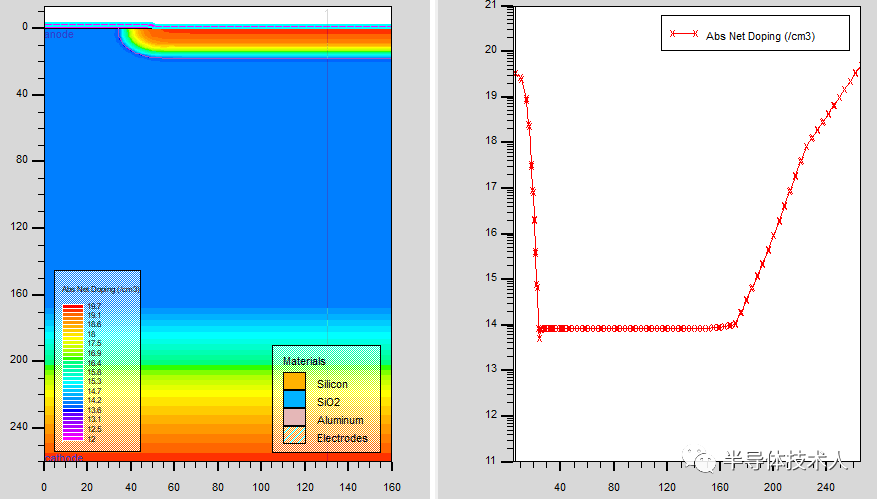
According to the requirements of actual electrical parameters, at room temperature of 25°C, when the test current IR=5μA, the device The reverse repetitive peak voltage (VRRM) needs to be higher than 1200V. In order to ensure the reliability of the device structure design, a 10% margin is considered for the breakdown voltage index, that is, the breakdown voltage design target value is 1320V. Figure 2 shows the effect of the simulated resistivity of N-type single crystal silicon on the breakdown voltage of the device. During the simulation process, the minority carrier lifetime of the substrate is 10 μs, the thickness of the high-resistance N-type region is 180 μm, and the surface concentration of the P+ region is 5E19cm-3 , with a junction depth of 10.5 μm. When the resistivity of N-type single crystal silicon is greater than 45Ω.cm, the breakdown voltage of the device is about 1400V, which meets the design requirements. Fig. 3 shows the influence of the thickness of the high-resistance N-type single crystal silicon on the breakdown voltage of the device obtained through simulation.
In the simulation process, the minority carrier lifetime of the substrate is 10μs, the resistivity of the original single crystal silicon is 45Ω.cm, the surface concentration of the P+ region is 5E19cm-3, and the junction depth is 10.5μm. When the thickness of high-resistance N-type monocrystalline silicon is ≥90 μm, the breakdown voltage of the device is about 1350V, which meets the design requirements. The basic structural parameters of the device are selected as follows: the crystal orientation of the original N-type single crystal silicon wafer is