-
Mail us
sale@tiger-transformer.com -
Phone us
(+86)15155183777 -


Mail us
sale@tiger-transformer.comPhone us
(+86)15155183777
1
Characteristics of SiC Schottky barrier diodes, and comparison with Si diodes
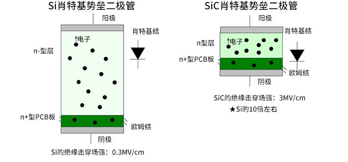
We start from The structure of SiC Schottky barrier diode (hereinafter referred to as "SBD") is introduced. As shown in the figure below, in order to form a Schottky barrier, semiconductor SiC is joined to a metal (Schottky junction). The structure is basically the same as that of Si Schottky barrier diodes, and its important feature is also high-speed characteristics.
The characteristic of SiC-SBD is that it not only has excellent high-speed performance but also realizes high withstand voltage at the same time. In order to improve the withstand voltage of Si-SBD, it is only necessary to thicken the n-type layer in the figure and reduce the carrier concentration, but this will bring about problems such as increased resistance and higher VF loss, which cannot be practically applied. Therefore, the withstand voltage of Si-SBD 200V is already the limit. SiC has an insulation breakdown field strength 10 times higher than that of silicon, so it can not only maintain practical application characteristics but also withstand high voltage.
SiC -SBD and Si-PN junction diodes
Si diodes are PN junction diodes (called "PNDs") that cope with withstand voltages higher than SBD. The figure below shows the structure of a Si-PN diode. In SBD, only electrons move and current flows, while in PN junction diodes, current flows through electrons and holes (holes). By accumulating minority carrier holes in the n-layer, the resistance value is lowered, so as to achieve high withstand voltage and low resistance value at the same time, but the turn-off speed will be slower.
Although FRD (Fast Recovery Diode) utilizes PN junction diode to improve speed, but nevertheless, trr (reverse recovery time) characteristic is inferior to SBD. Therefore, trr loss is a major research item for high withstand voltage Si PN junction diodes. At this time, one of the problems is that the switching power supply cannot cope with the high-speed switching frequency.
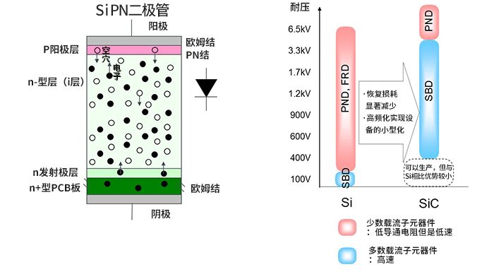
Top right The figure shows the coverage of Si SBD, PND, FRD and SiC-SBD withstand voltage. It can be seen that SiC-SBD basically covers the withstand voltage range of PND/FRD. SiC-SBD can achieve high speed and high withstand voltage at the same time. Compared with PND/FRD, Err (recovery loss) can be significantly reduced, and the switching frequency can also be increased. Therefore, small transformers and capacitors can be used, which contributes to the miniaturization of equipment.
2
Comparison of reverse recovery characteristics between SiC-SBD and Si-PND
The direction recovery characteristic is a basic and important parameter of diodes, especially high-speed diodes. Therefore, it is not only necessary to compare the value of trr, but also to understand its waveform and temperature characteristics, which is helpful for effective use of diodes.
First of all, reverse recovery or recovery refers to the phenomenon that when a diode is in a reverse biased state, it cannot be completely turned off immediately, and sometimes reverse current occurs. trr is the flow time of its reverse current. Let's look at the reasons for this and the actual characteristics.
Simply put, the difference in speed and reverse recovery characteristics of trr is due to the difference in diode construction. This requires talking about electrons and holes moving in semiconductors. First use the waveform diagram to understand the difference in reverse recovery characteristics between SiC-SBD and Si-PND. 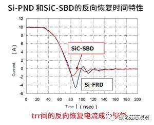
The waveform diagram above shows the current and time during reverse recovery of SiC-SBD and high-speed PND, that is, Si-FRD. It can be seen from the waveform diagram that the red SiC-SBD has less reverse current and shorter trr. By the way, this characteristic needs to be investigated because of the loss of reverse current.
Reverse recovery time characteristics of Si-PND and SiC-SBD
Here, we introduce the cross-sectional view of each diode. The figure below shows the movement of electrons and holes when the bias of Si-PND is switched from forward bias to reverse bias.
When forward biased, carriers are injected, and current flows through the recombination of holes and electrons. If it is reverse biased, the n-layer holes (minority carriers) will take some time to return to the p-layer, and current will flow until they return completely (a part disappears due to lifetime). This is the reverse recovery current. 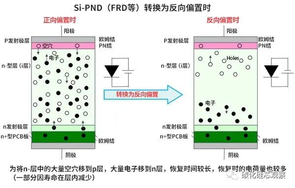
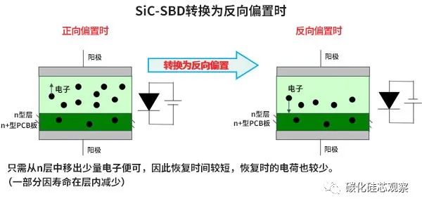
The second picture is SiC - Schematic of the SBD when converted to reverse bias. There is no PN junction due to the Schottky barrier structure, so there are no minority carriers, and the majority carriers (electrons) in the n layer only need to return when reverse biased, so only a small reverse recovery time is required , its turn-off time is significantly shorter than that of PND.
This difference in reverse recovery time is due to the diode structure. Therefore, the reverse recovery of Si-SBD is also high speed. However, the Si-SBD current withstand voltage limit is about 200V, and it cannot be used at a voltage higher than that. On the other hand, if SiC is used, a high withstand voltage SBD exceeding 600V can be produced. This is one of the great advantages of SiC-SBD.
The data on the temperature dependence and current dependence of the reverse recovery characteristics are shown below. 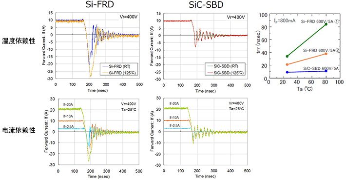
The oscillograms and graphs in the upper section represent different reverse recovery characteristics at different temperatures. When the temperature of Si-FRD rises, the carrier concentration also rises, so a corresponding reverse recovery time is required. As the room temperature increases, the reverse current and trr will also increase. On the other hand, SiC-SBD basically has no change in reverse current characteristics because SiC itself has basically no temperature dependence. The difference in trr was made in the upper right graph, and by comparing the two Si-FRDs, it was found that the trr of SiC-SBD basically has no temperature dependence.
The waveform diagram in the lower row shows the relationship with the forward current IF at the time of forward bias. It can be observed from the waveform diagram that SiC-SBD is hardly affected.
Finally, although it is stated that SiC-SBD has almost no reverse current, it can be clearly seen from the waveform diagram that SiC-SBD is much less than Si-FRD, but it is not at all. This is due to the effect of the parasitic junction capacitance in the diode. Therefore, compared with Si-PND, the reverse current of SiC-SBD is not zero, but significantly reduced.
Reviewing Editor: Liu Qing