-
Mail us
sale@tiger-transformer.com -
Phone us
(+86)15155183777 -


Mail us
sale@tiger-transformer.comPhone us
(+86)15155183777
Digital circuits are increasingly used due to their outstanding features such as high stability, high reliability, programmability, ease of design and economy. It is a common development trend of current electronic information systems to adopt digital processing methods. Similarly, digitization will also be a development trend of IGBT drivers. This chapter takes the design of digital IGBT drive protection circuit as an example to introduce the realization of high-power IGBT drive protector.
Overall scheme design of digital drive protector
The design scheme of IGBT drive protector includes the design of power circuit, drive, signal isolation and protection schemes, which can be adopted according to different application requirements Different design options.
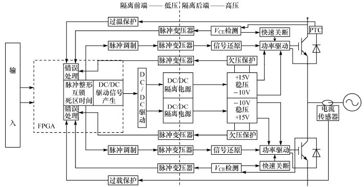
Figure 1 IGBT drive protection scheme for pulse transformer isolation< /p>
Figure 1 shows the IGBT drive protection scheme using pulse transformer for signal isolation (Wang Lihu, 2012). The system solution is mainly divided into the low-voltage part of the isolated front end and the high-voltage part of the isolated rear end. The back end is connected to the IGBT module by crimping through the physical interface, which mainly includes the following parts: power drive, VCE detection part, short circuit detection and fast shutdown, undervoltage detection and +15V and -10V isolated power supply. The front end mainly includes digital control part (FPGA or CPLD), over-temperature signal processing, current signal processing, isolated power drive and overload protection monitoring. The digital control part includes error handling, pulse shaping (short pulse suppression), interlock, dead time, and drive signals for DC/DC isolated power supplies. The input signal is provided by the external control unit. The external signal first enters the digital processing part. After short pulse suppression, interlock, dead zone setting and other processing are performed internally, it is transmitted to the back end through pulse modulation and pulse transformer, and the back end passes through the pulse Reshape and restore the driving signal, because the driving power of the driving signal is not enough to drive the high-power IGBT module, so it is necessary to increase the driving power through power amplification, so that the IGBT module can be turned on and off within the required time, which is the design of the driving part .
The power supply required for power amplification comes from the front end through DC/DC isolated power supply. During the working process of IGBT, if the power supply required for power amplification is undervoltage, it will cause the IGBT to fail to switch at the required speed , lead to wrong switching, and even cause IGBT through damage, so the upper and lower power supplies need to have undervoltage detection to ensure the stability of power amplification. The detection signal is transmitted to the digital section of the front end for processing through isolation. After the system detects the short-circuit signal of the IGBT through the VCE, it first shuts off the driving signal quickly at the back end of the isolation, and then transmits it to the front end through the isolation, and enters the digital part for processing. After the temperature detection and overload detection are detected by the sensor, they are directly input to the front end, and the analog signal is sent to the external client through signal processing, and the error signal is sent to the digital part for related processing. The DC/DC isolated power supply adopts the full bridge mode, and the signal output by the digital part is not enough to drive the main circuit of the DC/DC full bridge conversion, so the isolated front end of the DC/DC isolated power supply needs a power drive part.
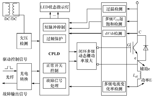
Figure 2 Fiber-isolated IGBT drive scheme
Figure 2 shows a high-power IGBT digital programmable driver using optical fiber for signal isolation (Wang Liangliang, 2015). The core of the driver is a digital control unit CPLD, in addition to the following parts: DC/DC converter with high isolation voltage, signal isolation transmission part, closed-loop multi-level dynamic gate drive part, various fault detection And protection part and status feedback part. The digital control unit CPLD includes the following modules: short pulse suppression module, input signal overfrequency protection module, normal switch signal control module, various fault signal detection modules, fault soft shutdown control module and corresponding status indicator light control module. A variety of fault detection and protection parts include the following functions: two-level current change rate dI/dt, multi-level VCE desaturation detection, IGBT over-current, over-temperature detection and protection, drive power supply under-voltage detection and protection.
The drive control signal (PWM) is provided by the external control unit, which first enters the CPLD digital processing unit through optical fiber isolation transmission, and after internal processing such as short pulse suppression and overfrequency protection, it controls the closed-loop multi-level dynamic The gate power amplification part makes the IGBT turn on and off reasonably and correctly according to the actual demand, which is the driving part of the whole module.
When the IGBT has a fault signal, the fault detection and protection part will send the detected information to the CPLD. After the CPLD confirms the authenticity of the fault, it will issue a corresponding protection command to protect the IGBT from damage, and at the same time, it can feed back the running status of the IGBT to the external controller in real time, which is convenient for users to use. The power required by the entire drive and protection circuit comes from the high isolation voltage DC/DC converter, which is the energy source to ensure the safe and reliable operation of the IGBT.
Drive circuit design
When the IGBT is turned on, the drive circuit needs to provide a certain amplitude of positive turn-on voltage to charge the gate capacitor to saturate the IGBT. When turning off, a certain magnitude of off voltage is provided to extract the charge stored in the gate capacitance, so that the IGBT is in the off state. Therefore, the digital chip can be used to control the on-off of the corresponding power devices to change the flow direction of the loop current and realize the turn-on and turn-off operations of the IGBT (Wenyang et al., 2016).
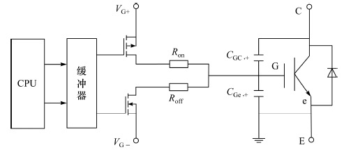
Figure 3 Simple digital drive circuit
Figure 3 is a simple digital drive circuit. The signal sent by the control chip CPU enters the buffer and then controls the turn-on and turn-off of the switch tube, so as to obtain the positive and negative voltages required for the turn-on and turn-off of the IGBT.
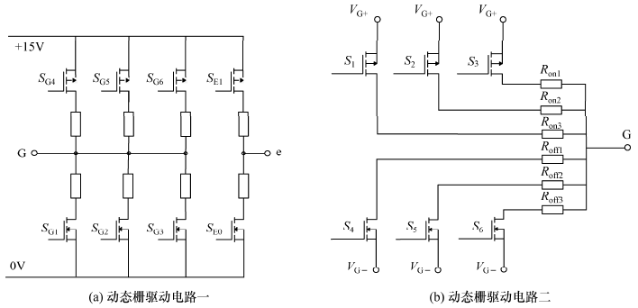
Figure 4 Digital dynamic gate drive structure
With the continuous development of IGBT drive technology, researchers have proposed a dynamic gate drive structure that can optimize IGBT switching characteristics. Figure 4 is a digital dynamic gate drive structure, in which Figure 4(a) and Figure 4(b) work roughly the same. During the switching process of the IGBT, according to the switching characteristics of the IGBT, the on-off of the corresponding switching tube is controlled to change the size of its gate drive resistance, adjust the on-off rate of the IGBT, and optimize its switching characteristics.
Moreover, due to the programmability of the control chip, when the driving power is large enough, the on-off combination of each switch tube can be adjusted to realize different manufacturers, different voltage levels, and different current levels. And the switch control of different types of IGBTs greatly improves the compatibility of the driver.
In addition, the drive structure shown in Figure 4(b) only needs a single drive power supply to meet the drive voltage requirements for turn-on and turn-off. When the IGBT is to be driven to turn on, the emitter e terminal is connected to 0V potential, the gate G is connected to +15V potential by controlling the on-off of the switch tube, and a +15V turn-on driving voltage is generated between the gate and the emitter. When the IGBT is to be driven to turn off, the emitter e terminal is connected to the +15V potential, the gate is connected to the 0V potential, and a -15V off voltage is generated between the gate and the emitter. This is beneficial to reduce the design cost of the power supply and reduce the size of the driver (Wang Liangliang et al., 2016a).
Digital protection circuit design
The protection operation of IGBT mainly includes voltage fault protection, current fault protection and temperature fault protection, and the output signal of the detection circuit corresponding to these faults Usually it is a digital signal. Therefore, the fault signal can be directly sent to the digital programmable chip for processing and analysis, and different protection operations can be configured according to different fault types.
When the detection circuit detects a fault signal and feeds it back to the digital protection circuit, the protection circuit first needs to screen the fault signal to determine whether it is a valid error signal, so as to avoid false protection. For how to confirm the fault signal, the principle of counter counting and then judgment is generally adopted. Assuming that the error signal is low-level effective, after receiving the low-level, if the low-level duration is less than the fault confirmation time tc, the level is considered to be Interference level, the level greater than the fault confirmation time tc is the effective level. The confirmation time is different for different types of faults, and the specific time depends on the electrical characteristics of this type of fault.
For different types of faults, the control strategies for shutdown protection are also different. For example, when a short-circuit fault occurs in an IGBT, the collector current IC rises rapidly to several times the rated current. At this time, it is necessary to perform a soft turn-off operation on the IGBT, so as to avoid excessive turn-off surge voltage caused by too fast a turn-off rate. High, causing secondary damage to the IGBT. At the same time, for different types of faults, the response time of the shutdown protection is also different. Usually, after detecting the IGBT fault signal, the driver will quickly identify and respond to the fault signal, and turn off the IGBT in the fault state. However, for the overload and overcurrent fault of the IGBT, since the current value is 1.2 to 1.5 times the rated value during overload, the overload and overcurrent does not need to respond quickly, and a short period of overload operation is allowed (Wang Liangliang et al., 2016b).
Figure 5 is an implementation method of a digital protection circuit. This strategy sets different shutdown protection methods and response time of protection actions for different types of fault signals. When the fault signal is input to the main control chip, the control chip will judge the type of fault. If it is an overload fault, the authenticity of the fault signal is screened. After the fault confirmation time tc1, if the fault state still exists, the IGBT is turned off for protection. The collector current is low during an overload fault, so only normal shutdown is required. Aiming at the problem of large turn-off stress during short-circuit overcurrent fault protection, this strategy uses soft turn-off to avoid secondary damage caused by turn-off overvoltage.
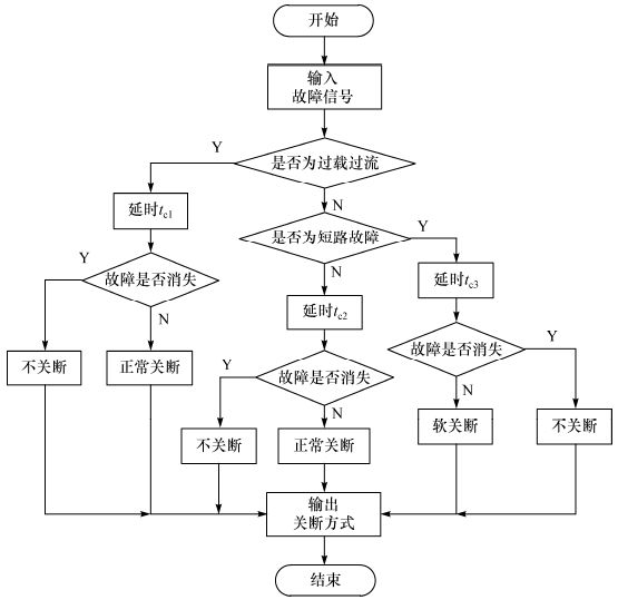
Figure 5 A digital protection circuit implementation method
Another advantage of the digital drive is its scalability. Usually, after the IGBT enters the fault state, the driver needs to feed back the control signal to the main control terminal, and the definition of the feedback signal in different application places is different, so it is difficult for the general driver to be compatible on this point. The advantage of the digital drive lies in its programmability, and it only needs to slightly modify its control program on the basis of the existing hardware circuit to achieve the corresponding goal.