-
Mail us
sale@tiger-transformer.com -
Phone us
(+86)15155183777 -


Mail us
sale@tiger-transformer.comPhone us
(+86)15155183777
Silicon carbide (SiC) components have significant Advantages, so many applications can benefit from using SiC devices. But parametric design with SiC devices is not a straightforward process. Whether developing a new product or upgrading a previous design, it is best to simulate and optimize devices early in the design phase, before topology and device selection are determined.
SpeedFit design simulation software is an online system-level circuit simulation software based on PLECS, designed to assist in several key areas, such as inter-device comparison and topology comparison, parallel design configuration, thermal management, and evaluation Hardware properties (such as semiconductor losses and inductor/transformer waveforms) to help fit specific circuit topologies or chips group.
** #1 **
SpeedFit Switching and Conduction Loss Modeling
For SiC MOSFET For u>, three typical loss sources can be analyzed. The first is the loss at turn-on (Eon), the second is the loss at turn-off (Eoff), and finally the conduction loss at "on" (denoted Pconducttion). Therefore, the total power loss can be expressed as:
Ptotal = ((Eon + Eoff) × Fsw) + Pconduction
Figure 1 shows the gate signal Pulse and relationship of Vds, Ids and Ploss to signal in switching state.
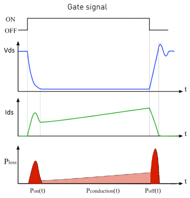
▲ Figure 1: SiC MOSFET switch and Power Loss Waveform
In the on state, the conduction power loss depends on the junction temperature (TJ) and the drain current (ID). The curves of different VDS and ID at different temperatures are saved in the lookup table, and the "turn-on" voltage can be obtained by interpolation. Due to the very low leakage current, the power loss in the off state is negligible.
Switching losses depend on VDS, IDS, TJ and external gate resistor (RG). A three-dimensional lookup table of switching losses (as a function of ID, off-state voltage, and temperature) is used to determine the Eon and Eoff values at each switching event. These values are then adjusted according to the selected external gate resistor (RG). When measuring the overall average total loss of the device, the general goal is to calculate the overall conduction and switching energy losses during one switching cycle, and then output it as an average power pulse during the next cycle. This can be achieved using a module that takes probe measurements and observes the periodic average (conduction loss) and periodic pulse average (switching loss), after which the results are averaged (see Figure 2).
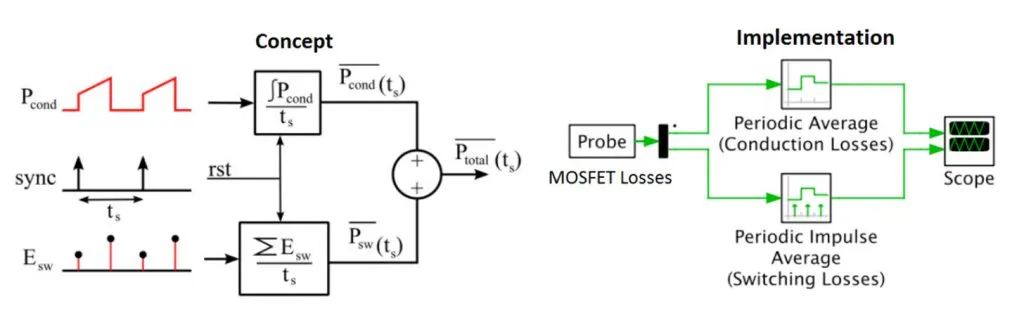
▲ Figure 2: Determination of overall device average Conceptual Diagram and Implementation of Losses
SpeedFit simulateselectrical and thermal characteristics, then uses a lookup table to determine the losses, and add them to the thermal circuit (including the heatsink). For the circuit, the simulation calculates the current and voltage applied across the switch, then feeds the data into a loss lookup table after each switching event. In the thermal domain, TJ is estimated and updated based on previous cycle and current cycle losses. The obtained result TJ is fed back to the look-up table for the next cycle. Figure 3 shows this simulation.
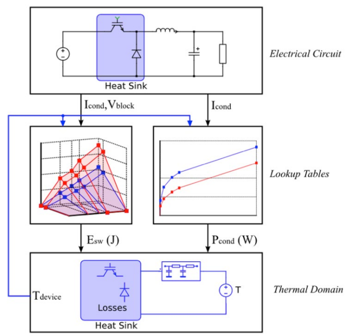
▲ Figure 3: SpeedFit simulates electrical and Thermal Model
** #2 **
How to Run Setup and Simulation
When Using SpeedFit to Get Started During simulation, the user needs to select Application (application), Input (input) operating parameters and topology, select Device (device ), set the Thermal parameter, run Simulation, and print the Summary ) report. We provide user guides with practical tips and range limits for each topology.
When selecting Application, there are several converter types to choose from (DC/DC, AC/DC and DC/AC). For multi-stage converters where the active front end is followed by a CLLC DC/DC stage, each stage should be simulated separately.
When Input (input) is running parameters (see Figure 4), first select the required topology (if known), or directly enter the input/output parameters to view the matching circuit. The parameters the user sees may change depending on the topology selected, and the "resonance-based" topology has buttons that automatically import suggested resonator component values for easy configuration.
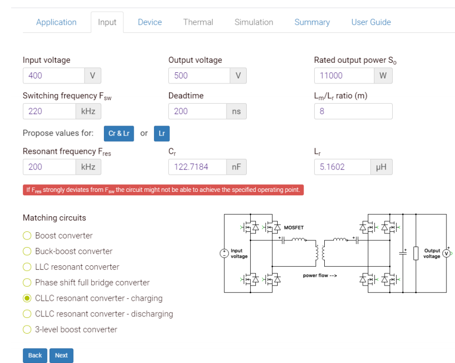
▲ Figure 4: SpeedFit input operating parameters and Select Topology Window
Once the voltage and current ratings have been determined, the Device tab will display a short list of suggested devices with all optional A longer/complete list of devices (MOSFETs, diodes, modules). During this process, the user can adjust the number of devices connected in parallel as well as the gate resistance. Also, when using discrete MOSFETs in AC/DC or DC/AC applications, a Schottky diode can be added in parallel with the MOSFETs to reduce losses during switching.
The internal thermal junction resistance (Rth,JC) is automatically included when setting the Thermal parameter; however, the user needs to enter the thermal interface resistance (Rth,ch). Interface resistance is calculated every time a switch is made. A power module with multiple switch positions will contain two, four or six or more Rth,ch in parallel depending on the number of switches in the module. Thermal resistance values can be variable or fixed, depending on the application. A variable heat sink can be modeled as a thermal impedance (Tamb) to the surrounding environment and includes a time constant. If the fixed heatsink option is selected, the heatsink temperature must be specified. For topologies that include primary and secondary side SiC devices, separate (but identical) heat sinks are required for each side.
Simulate tab displays the user-specified topology, heatsink configuration, and key parameters (see Figure 5). Passive component parameters in the circuit can be tuned to the design prior to simulation to tune the design to match the application and further optimize the results. After simulation, the waveforms and source voltage, load voltage, input current, load current, and diode/MOSFET voltage and current are displayed. The system overview table shows power, switching frequency, efficiency, while the device overview table shows losses and estimated junction temperature. The losses shown in the device overview table are the sum of losses for all such devices. For example, in Figure 5, the sum of the losses of all 4 primary side SiC MOSFETs is 54.54 W.
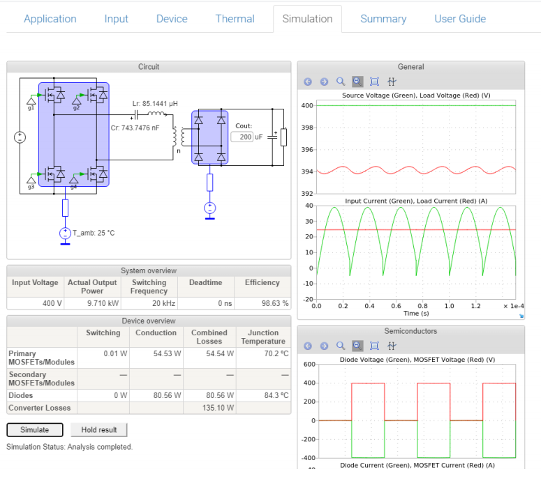
▲ Figure 5: SpeedFit simulation page display Topologies, Waveforms, and Multiple Digital Readouts
Users can run additional iterations of the same topology to compare results and optimize designs. First, the user clicks the "hold result" button in the simulation tab to save the previous result for reference, then enter another operating point, or evaluate an alternate device, and re-simulate the new conditions.
Finally, the Summary tab provides detailed results for multiple simulation runs (called "variables") and displays side-by-side comparison results. Also the User Guide tab provides a table of operating limitations for each topology and explains the parameters in each tab. Example data are also provided, which can be used under different thermal conditions and can provide a good first approximation for designing new systems where the thermal impedance has not yet been determined.
** #3 **
SpeedFit Application Example
Let's run a sample application: 45 kW Three Phase Inverter The converter is air-cooled, the power supply is 800 V busbar power supply, the output is 480 V, and the switching frequency is 10 kHz. The goal is to evaluate Wolfspeed's WolfPACK SiC MOSFET half-bridge modules as well as discrete SiC MOSFETs.
In this example, four options (two discrete and two modular) with multiple possibilities were easily evaluated within minutes, all with >99% efficiency. Solution includes:
2 × C3M0016120K (16 mΩ TO-247-4)
2 × C3M0021120K (21 mΩ TO-247-4)
CAB011M12FM3 (11 mΩ FM3 WolfPACK)
CAB016M12FM3 (16 mΩ FM3 WolfPACK)
While weighing mounting size, temperature margin, power density/layout and cost etc. These results can inform a complete system architecture evaluation when considering these factors. Figure 6 shows the simulation results and demonstrates how quick and easy it is to compare different schemes involving discrete and modular MOSFETs.
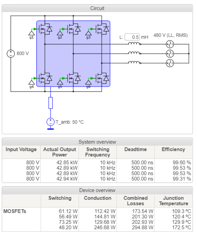
▲ Figure 6: 45 kW three-phase Example of Inverter Simulation Results
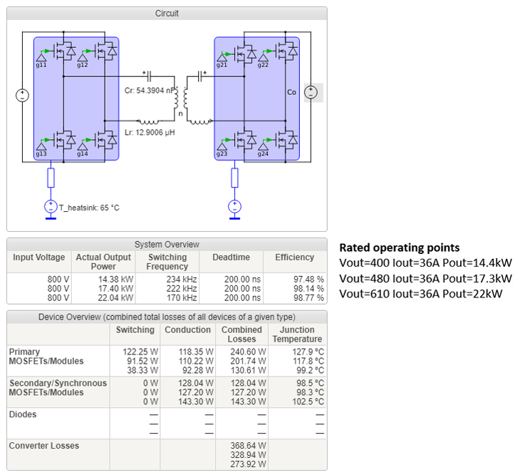
Another example is a bi-directional CLLC DC/DC on-board charging system operating at 22 kW (which can be used in EV charging applications). Since it will be used in electric vehicles, the input voltage is between 380 - 900 VDC and the output should be between 480 - 800 VDC. This example tests three power levels to evaluate efficiency and junction temperature. The three outputs are 400 V, 480 V and 610 V, all operating at an output current of 36 A. The chosen topology is a full-bridge CLLC resonant converter operating between 135 - 250 kHz. The plan here is to optimize the design by running the simulation, looking at the results, and making fine-tuning as needed. A concrete example can be seen in reference design CRD-22DD12N.
In the first run on the "Input" tab (see Figure 7), the user enters the input voltage, output voltage, output power Lm/Lr, Fsw and Fres. It is recommended to start with Fsw = Fres (190 kHz). The rest of the values will be filled in automatically.
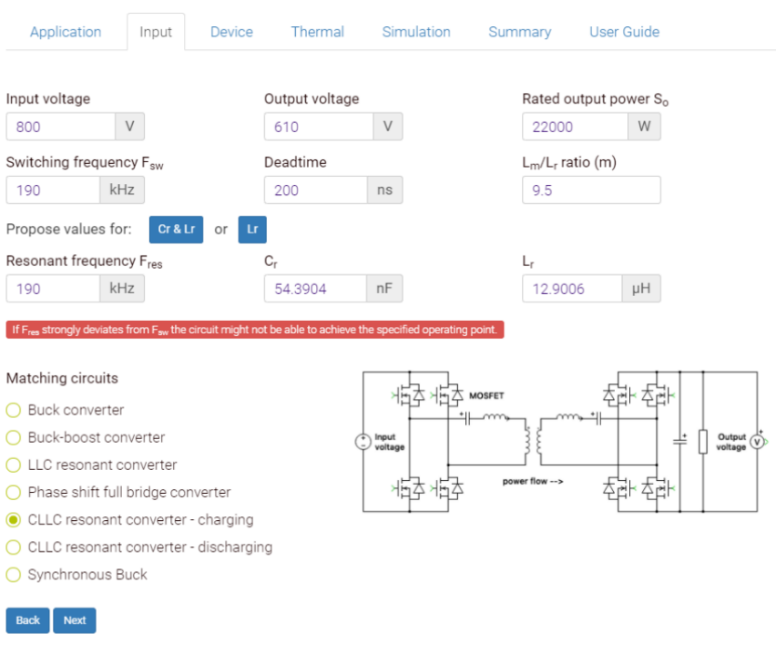
▲ Figure 7: 22 kW CLLC DC /DC Converter ****Example in "Input"
Tab
In "Device )" tab, select 32 mΩ 1,200 V MOSFETs for both primary and secondary sides for maximum efficiency. A gate resistance higher than the default setting will result in increased switching losses, but will allow design flexibility during the test phase. Rg should be determined based on circuit experiments to achieve the desired voltage overshoot margin and EMI performance.
For thermal performance, choose an isolated liquid-cooled radiator capable of maintaining the radiator temperature at 65 ˚C. High performance aluminum nitride spacers coated with thermal grease on both sides provide good thermal isolation and low thermal resistance (0.6 K/W as shown in user guide) for TO-247 solutions.
During the simulation, the results of the first run showed that the output power was too low. Based on the basic principle of CLLC converters, a lower operating frequency increases the output voltage (and output power), so the simulation was rerun with a lower switching frequency (down to 170 kHz). This can increase the output power to an acceptable value and provides a usable solution (as shown in Figure 8).
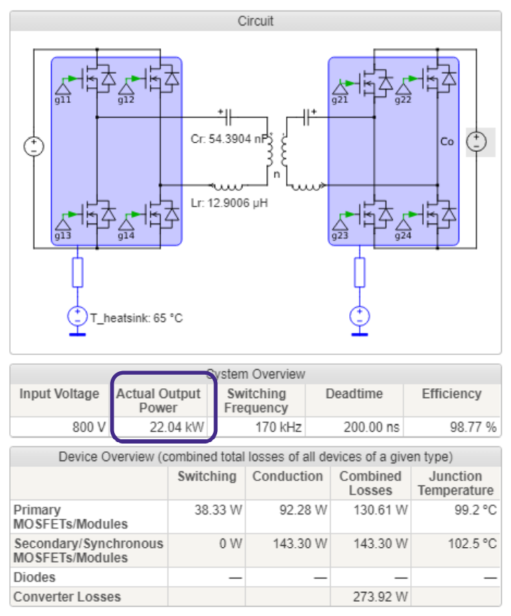
▲ Figure 8: CLLC DC/DC Example of simulation results from a second run of a converter
In this example, the user can compare the results of several additional operating points: by clicking on the "hold result" option, Then go back to the Input tab and enter new data. After re-simulation, adjust Fsw if necessary to fine-tune the desired output, then repeat the process for the remaining operating points. A summary is generated containing per-simulation results for adjacent case comparisons. This method can also be used to verify safe operating temperatures under all operating conditions.
▲ Figure 9< /p>
** #4 **
Conclusion
After simulating multiple configurations and obtaining optimization results, designers can significantly benefit. SpeedFit is an easy-to-use software based on the PLECS platform, which can replace time-consuming manual comparison and calculation of data sheets. Designers can find the right SiC MOSFET and SiC diode, evaluate performance (and losses) at different operating points, determine the thermal requirements of the system, evaluate many different types of topologies and obtain waveforms to optimize capacitors and electromagnetically related designs, which benefit significantly.