-
Mail us
sale@tiger-transformer.com -
Phone us
(+86)15155183777 -


Mail us
sale@tiger-transformer.comPhone us
(+86)15155183777
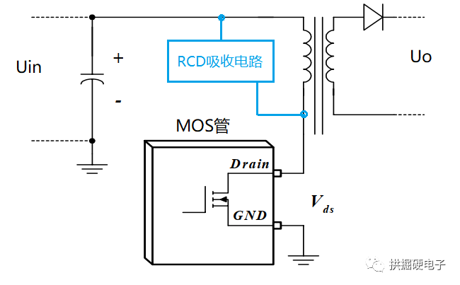
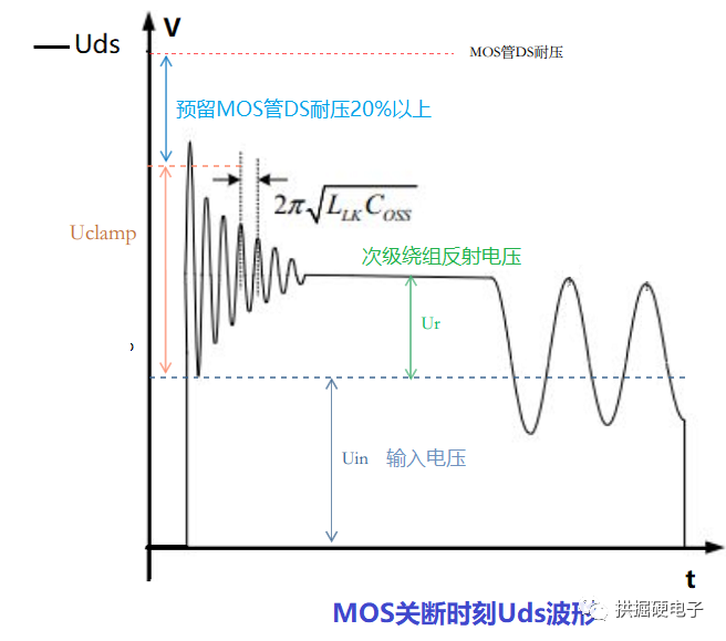
When the MOS tube of the flyback switching power supply is turned off, the energy stored in the leakage inductance of the primary winding of the transformer cannot be transferred to the secondary winding, and the leakage inductance of the primary winding and the parasitic capacitance of the MOS tube generate a resonant voltage waveform. This resonant voltage peak is superimposed with the reflected voltage of the secondary winding and the input voltage of the power supply, and is loaded to both ends of DS of the MOS tube. If the loading voltage exceeds the withstand voltage of the MOS tube, the MOS tube will be damaged. If it is loaded under the withstand voltage of the MOS tube, but close to the withstand voltage of the MOS tube, it will affect the service life of the MOS tube. The function of the RCD absorption circuit is to suppress the peak of the resonant voltage, leaving at least 20% voltage margin for the withstand voltage of the MOS tube, so as to avoid damage to the MOS tube or affect the service life of the MOS tube. In addition, the RCD snubber circuit suppresses the resonance voltage oscillation, which is beneficial to EMI.
The cause of the resonance wave
Analyze the superimposed voltage waveform. According to the principle of RLC series circuit, the period of the resonant voltage waveform is 2π×(Llk×Coss)^0.5, and the resonant frequency is the reciprocal of the period, where Llk is the leakage inductance of the primary winding, and Coss is the MOS tube parasitic capacitance.
In the circuit, the inductor and capacitor series resonance model is as follows . At the resonant frequency, the impedances of the inductor and the capacitor cancel each other out, and there is only the parasitic resistance of the line in the entire loop. The inductor charges the capacitor, and then the capacitor charges the inductor. The energy circulates between the two, and the energy is difficult to consume, forming a resonance voltage. waveform.
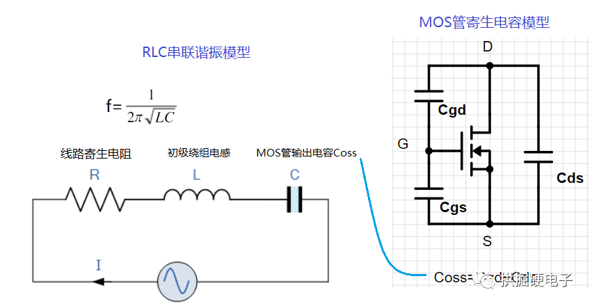
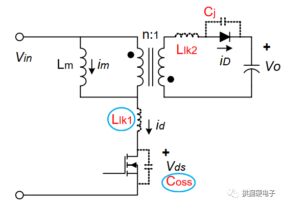
The key component parasitic parameter model of the flyback switching power supply is as follows , here only focus on the primary winding leakage inductance Llk1, MOS output capacitance Coss.
Working principle of RCD absorption circuit
There are other circuit forms for absorbing MOS tube voltage spikes, but RCD absorbing circuits are the most commonly used in switching power supplies. The RCD absorption circuit is composed of a diode D, a resistor R, and a capacitor C, and its circuit structure is shown in the figure below.
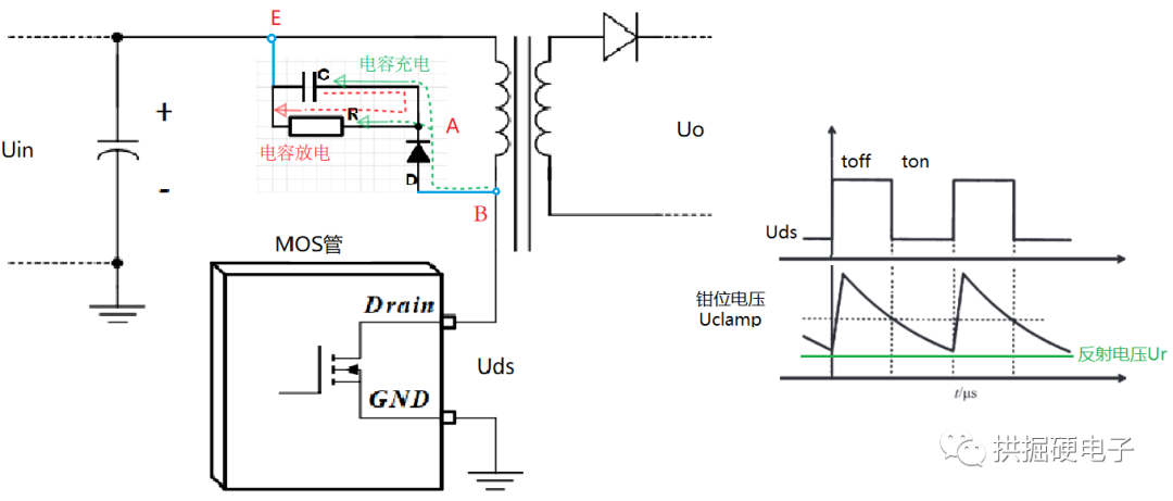
Combined with the schematic diagram, ignore the forward conduction of diode D pressure drop. When the MOS is turned off, the resonant voltage waveform generates a voltage spike at point B. At this time, UB is higher than UA (there is no voltage difference between the two ends of the capacitor C at the initial moment), then UB charges the capacitor C through the diode D. The essence of the Uds voltage increase is that the voltage generated by the transient current induction of the leakage inductance of the primary winding (the magnetic energy stored in the leakage inductance of the primary winding) charges the parasitic capacitance Coss of the MOS tube, and the charges at both ends of the parasitic capacitance Coss accumulate, and the voltage difference increases. When the diode D is turned on, since the capacitor C is much larger than the parasitic capacitance of the MOS tube, the capacitor C will share most of the current (this part of the current is originally charged to the parasitic capacitor Coss), so that the charging process of the parasitic capacitor Coss becomes Slow, so the capacitor C will suppress the Uds voltage spike. At the same time, the resistance R consumes the energy stored in the leakage inductance of the primary winding, so that the resonance waveform becomes stable as soon as possible.
During the time when the MOS tube is turned off, the clamping capacitor is quickly charged to the set clamping voltage, and the resonance voltage peak is lower than the clamping voltage (when the resonance voltage UB waveform begins to drop below UA , and keeps UB lower than UA, UB gradually falls back to Uin+Ur), and then the clamping diode is cut off, and the clamping capacitor C releases energy in the form of heat through the clamping resistor R. It should be noted that the discharge speed of the resistor R needs to be limited (meaning that the resistance value of the resistor cannot be selected too small) to ensure that the clamping voltage will not be lower than the reflected voltage, otherwise UB is smaller than UA (at this time UB=Uin+Ur, UA =Uin+Uclamp, Uclamp is gradually reduced by the resistance discharge), then the clamping diode is turned on, and the clamping resistor starts to consume the energy originally to be transferred to the secondary winding, which will reduce the power supply efficiency. In this way, when the MOS tube is turned off, the RCD snubber circuit absorbs the energy stored in the leakage inductance of the primary winding when the MOS tube is turned on, limiting Uds to not exceed UA.
In order to avoid the energy stored in the clamping capacitor C in the previous cycle from affecting the clamping action in the next cycle, it is required that the resistor R release all the energy on the clamping capacitor C before the next MOS is turned on. If there is no resistor R, the leakage inductance will charge the capacitor C in each cycle, so that the voltage across the capacitor C will continue to increase until the MOS tube or capacitor cannot withstand the high voltage and is damaged. Generally, the MOS tube switching period T=(2~4)×RC is required.
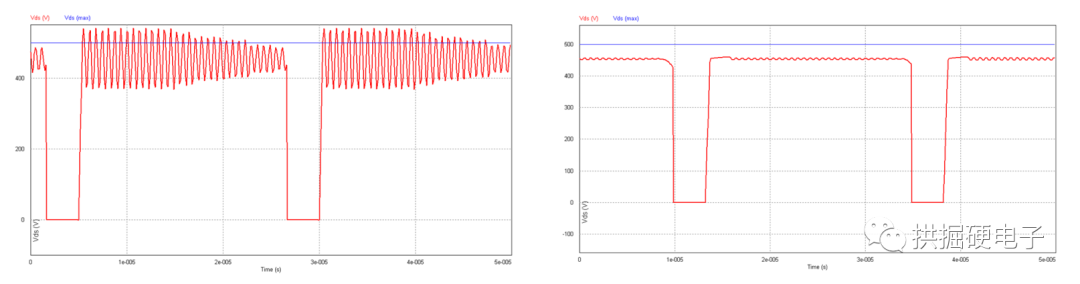
The figure below shows the comparison of MOS tube Uds test waveforms before and after the switching power supply is added with RCD circuit. The left picture is the test result of the circuit before adding RCD, and the right picture is the test result of the circuit after adding RCD:
Red: MOS tube Uds voltage, blue: MOS tube withstand voltage Uds max
Calculation of component selection
According to engineering experience, the maximum clamping voltage is usually set to be 22.5 times the reflected voltage, that is, Uclamp=(22.5) × Ur.
When the MOS tube is turned off, the leakage inductance energy of the primary winding is absorbed by the clamp capacitor. If the clamp capacitor capacity is too small, it will not be able to absorb all the energy, and Uds will continue to rise, causing No protective effect. Therefore, the selected clamping capacitor generally has a large capacitance. It is assumed that the Uclamp voltage remains unchanged (the voltage changes very little) when the clamping capacitor is charged. For the convenience of calculation, during the charging time of the clamp capacitor, it is assumed that the current of the leakage inductance flows into the clamp capacitor, and the current flowing to the resistor and the output capacitor of the MOS tube is ignored, and the forward conduction voltage drop of the clamp diode is also ignored.
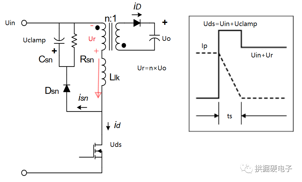
In a switching cycle, for the clamping capacitor Csn, the power absorbed by the capacitor is = capacitor energy storage per unit time = clamping voltage × capacitor average current × clamping time / switching cycle = Uclamp×0.5×Ip×ts×fs, where Ip is the leakage inductance peak current, ts is the clamping time, and fs is the switching frequency of the MOS tube.
In one switching cycle, for the leakage inductance Llk, ts=leakage inductance×leakage inductance current variation/leakage inductance voltage=Llk×Ip/(Uclamp-nUo), where nUo is the secondary Winding reflected voltage, instead of nVo in the figure. Among them, Usn is the capacitor clamping voltage, which replaces Vsn in the figure. Among them, Uclamp-nUo represents the voltage loaded on both ends of the leakage inductance. Among them, Ip is the peak current in the leakage inductance, and it is also the variation of the leakage inductance current within ts time. Where Llk represents the inductance value of the leakage inductance.
The power released by the leakage inductance=0.5×Llk×Ip²×ts×fs.
During a switching cycle, for the clamping resistor Rsn, all the power of the leakage inductance is dissipated by the resistor Rsn, and the power dissipated by the resistor = Uclamp²/Rsn.
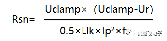
Combining the above three relational expressions, you can get clamp Bit resistor Rsn:
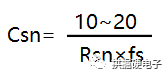
We need to set the clamp voltage The ripple voltage is set within a reasonable range, and it is generally considered appropriate that the ripple voltage accounts for 5% to 10% of the clamping voltage.
Ripple voltage=Uclamp/(Rsn×Csn×fs), the clamp capacitor Csn can be obtained:
Ultra-fast recovery diodes are selected for the clamping diodes, and the reverse withstand voltage of the diodes is selected based on the calculated MOS tube’s actual withstand voltage of more than 1.2 times.
In general, the RC snubber circuit is required to store energy during the off period of the MOS tube to suppress the rise of Uds. After that, it is required that the clamping voltage cannot be lower than the reflected voltage due to the resistance discharge. Release the energy in the clamp capacitor. When the MOS tube is turned off, Uds first oscillates up and then oscillates down. The clamp capacitor is charged first and then discharged. The whole process is relatively complicated. Because the RCD snubber circuit of the actual power supply is also affected by other parasitic parameters in the circuit, diode recovery characteristics, etc., after obtaining the preliminary parameters of the above RCD snubber circuit components, it is necessary to finally determine the design parameters according to the actual debugging situation.